Department of
Combinatorial Epitaxy
Head: Holger von Wenckstern
Combinatorial Epitaxy
Head: Holger von Wenckstern

Universität Leipzig
Fakultät für Physik und Geowissenschaften
Felix-Bloch-Institut für Festkörperphysik
Abteilung Kombinatorische Epitaxie
Linnéstraße 5
D-04103 Leipzig, Germany
Tel.: +49-(0)-341-97 32604
Fax: +49-(0)-341-97 32668
send e-mail message
Google Scholar
ResearchGate
ResearcherID
| PROJECTS | CV |
- Combinatorial pulsed laser deposition of thin films of functional oxides
- Electrical characterization of defect levels in wide bandgap semiconductors
- Transport phenomena of oxide heterostructures (2DEGs)
- Device characterization and optimization
e.g.: solar cells, UV-photodetectors, rectifiers, FETs, high-power devices... - Amorphous oxide semiconductors for flexible electronics
- Transparent p-type semiconductors
Recent progress on epitaxial growth and characterization of group-III sesquioxides

The group-III sesquioxides, especially Ga2O3, have promising material properties for high-power applications, deep-UV and quantum-well infrared photodetectors. The alloy material system crystallizes in various polymorphs including the rhombohedral α-, the monoclinic β-, the orthorhombic κ- and the cubic bixbyite phase. In the last years we have used combinatorial material science to study properties of the group-III sesquioxides as function of alloy composition for the various polymorphs. The figure indicates the miscibility gaps for various crystal structures as indicated.
The plethora of scientific findings can be found in
A. Hassa, H. von Wenckstern and M. Grundmann
Progression of group-III sesquioxides: epitaxy, solubility and desorption
J. Phys. D: Appl. Phys. 54, 223001 (2021)
M. Budde, D. Splith, P. Mazzolini, A. Tahraoui, J. Feldl, M. Ramsteiner, H. von Wenckstern, M. Grundmann, and O. Bierwagen
SnO/β-Ga2O3 vertical pn-heterojunction diodes
Applied Physics Letters 117, 252106 (2020)
A. Hassa, P. Storm, M. Kneiß, D. Splith, H. von Wenckstern, M. Lorenz, M. Grundmann
Structural and Elastic Properties of α-(AlxGa1-x)2O3 Thin Films on (11.0) Al2O3 Substrates for the Entire Composition Range
Phys. Status Solidi B. doi:10.1002/pssb.202000394 (2020)
M. Kneiß, P. Storm, A. Hassa, D. Splith, H. von Wenckstern, M. Lorenz, M. Grundmann
Epitaxial Growth of κ-(AlxGa1-x)O3 Layers and Superlattice Heterostructures up to x = 0.48 on Highly Conductive Al-doped ZnO Thin Film Templates by Pulsed Laser Deposition
Phys. Status Solidi B. doi:10.1002/pssb.202000359 (2020)
C. Wouters, C. Sutton, L. M. Ghiringhelli, T. Markurt, R. Schewski, A. Hassa, H. von Wenckstern, M. Grundmann, M. Scheffler, M. Albrecht
Investigating the ranges of (meta) stable phase formation in (InxGa1-x)2O3: Impact of the cation coordination
arXiv:2008.04573 (2020)
A. Hassa, C. Wouters, M. Kneiß, D. Splith, C. Sturm, H. von Wenckstern, M. Albrecht, M. Lorenz, M. Grundmann
Control of Phase Formation of (AlxGa1-x)2O3 Thin Films on c-plane Al2O3
J. Phys. D: Appl. Phys. 53, 485105 (2020)
H. von Wenckstern, D. Splith, M. Purfürst, Z. Zhang, Ch. Kranert, S. Müller, M. Lorenz, M. Grundmann
Structural and optical properties of (In,Ga)2O3 thin films and characteristics of Schottky contacts thereon
Semic. Sci. Technol. 30, 024005 (2015)
R. Schmidt-Grund, Ch. Kranert, T. Böntgen, H. von Wenckstern, H. Krauß, M. Grundmann
Dielectric function in the NIR-VUV spectral range of (InxGa1-x)2O3 thin films
J. Appl. Phys. 116, 053510 (2014)
Ch. Kranert, J. Lenzner, M. Jenderka, M. Lorenz, H. von Wenckstern, R. Schmidt-Grund, M. Grundmann
Lattice parameters and Raman-active phonon modes of (InxGa1-x)2O3 for x < 0.4
J. Appl. Phys. 116, 013505 (2014)
Ultra-high performance, transparent electronic device building blocks based on zinc-tin-oxide
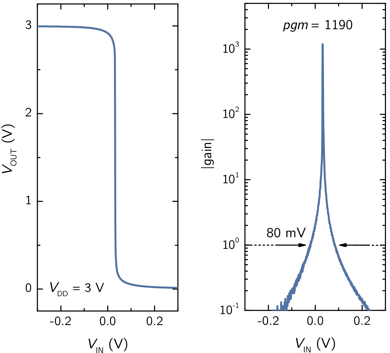
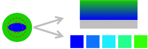
Zinc-tin-oxide (ZTO) is a promising amorphous, semiconducting oxide for sustainable, flexible electronics. It consists of abundant materials and devices can be fabricated entirely at room temperature. We demonstrate that metal-semiconductor field-effect transistors (MESFETs) and corresponding inverters exhibit remarkable performance for ZTO layers with a mean transmittance in the visible of 81%. The MESFET's current on/off ratio is six orders of magnitude and the full switching voltage is below 3V enabling mobile applications. Temporal and negative bias stress stability of device performance is demonstrated. Using the Schottky diode FET logic allows cascading of inverters for, e.g., ring oscillator applications. Here, the unpreceded performance of the MESFET-based inverters is highlighted. From the voltage transfer characteristics, a peak gain magnitude of 1190 and an uncertainty level of only 80mV (see figure) define record values for a driving voltage of only 3V.
Further information is available at:
O. Lahr, H. von Wenckstern, M. Grundmann
Ultrahigh-Performance Integrated Inverters Based on Amorphous Zinc Tin Oxide Deposited at Room Temperature
APL Materials 8, 091115 (2020), Editor's Pick
Oliver Lahr, Michael Bar, Holger von Wenckstern, Marius Grundmann
All-oxide transparent thin-film transistors based on amorphous zinc-tin-oxide fabricated at room temperature: Approaching the thermodynamic limit for sub-threshold swing
Adv. Electron. Mater. 6, 2000423 (2020)
Indium Gallium Oxide Alloys: Electronic Structure, Optical Gap, Surface Space Charge and Chemical Trends within Common Cation Semiconductors
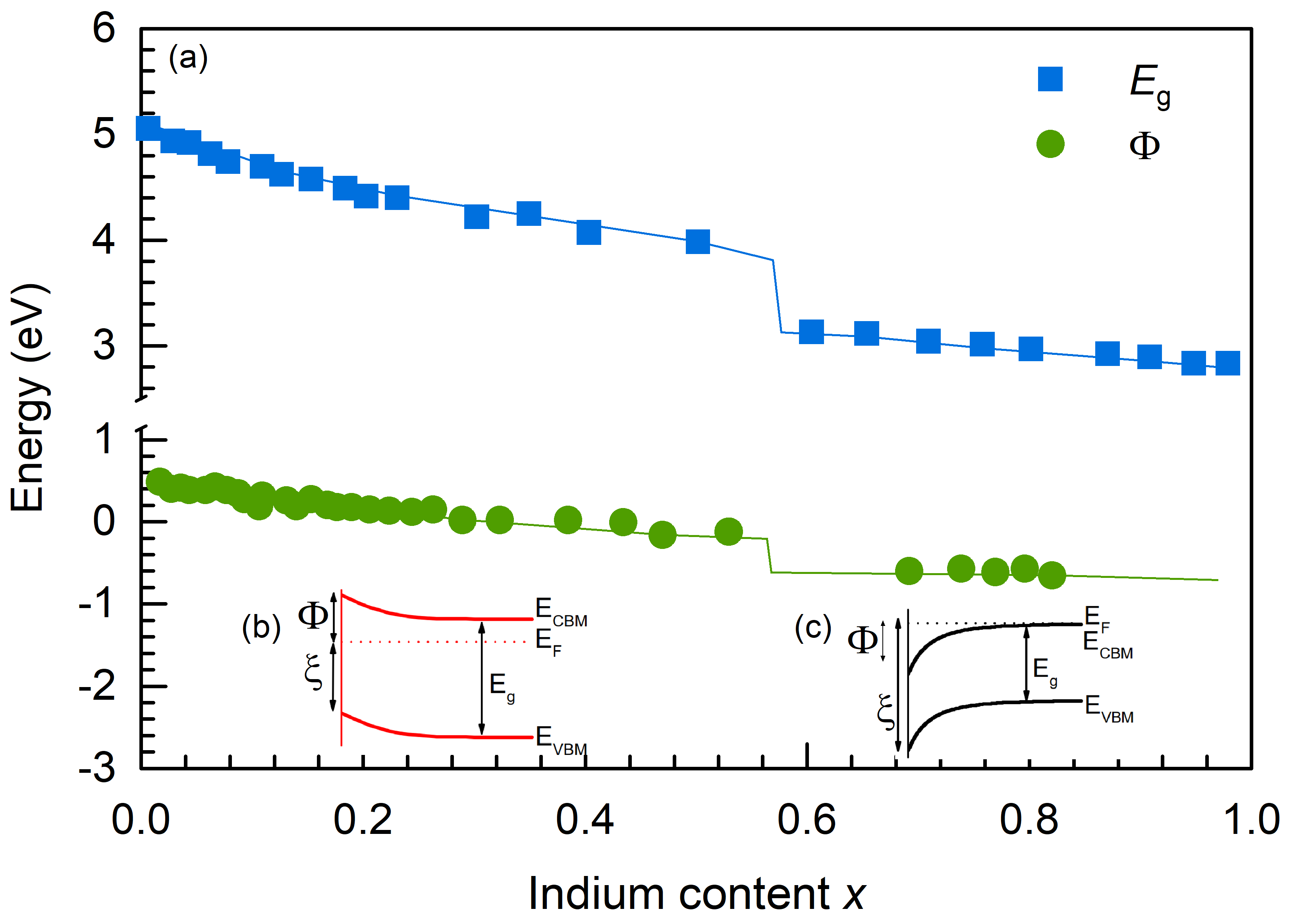
Within a collaboration of the University of Liverpool, the University of Oxford, the University College London, the Lawrence Livermore National Laboratory and Universität Leipzig the electronic and optical properties of a high-quality, continuous composition spread (InxGa1-x)2O3 thin film with 0.01 ≤ x ≤ 0.82 were characterized by X-ray diffraction, X-ray photoemission spectroscopy, optical transmission measurements and In2O3, Ga2O3 and InGaO3 by density functional theory (DFT). The sample crystallized in the monoclinic β-gallia structure on the Ga-rich side of the wafer, the hexagonal InGaO3 phase for similar Ga and In content and the cubic bixbyite phase for the In-rich sample part. As depicted in the figure, the optical bandgap gap decreases in accordance with increasing indium content even though different phases are present. The energy of the valence band maximum (VBM) with respect to the Fermi energy decreases slowly for low indium contents from about 4.3 eV for x = 0.01 to 4 eV for x = 0.5. For x > 0.5 a large decrease to 3.5 eV occurs as the crystal structure changes to the bixbyite phase. This is accompanied by a change of an upward surface band bending for low indium content to a downward bending and surface electron accumulation for bixbyite (In,Ga)2O3 as illustrated in the figure. DFT calculations reveal that the valence bands are dominated by oxygen 2p-states with contributions from the In 4d/Ga 3d states at the VBM. The conduction band minimum is In 5s/Ga 4s dominated with a strong O 2s contribution. Further, the electronic structure and band edge positions of In2O3, Ga2O3 and (InxGa1-x)2O3 alloys were understood in terms of their place within chemical trends of common-anion materials.
Further information is available at:
Jack E. N. Swallow, Robert G. Palgrave, Philip A. E. Murgatroyd, Anna Regoutz, Michael Lorenz, Anna Hassa, Marius Grundmann, Holger von Wenckstern, Joel B. Varley, and Tim D. Veal
Indium Gallium Oxide Alloys: Electronic Structure, Optical Gap, Surface Space Charge, and Chemical Trends within Common-Cation Semiconductors
ACS Appl. Mater. Interfaces 13, 2807(2021)
Experimental exploration of the amphoteric defect model by cryogenic ion irradiation of a range of wide band gap oxide materials
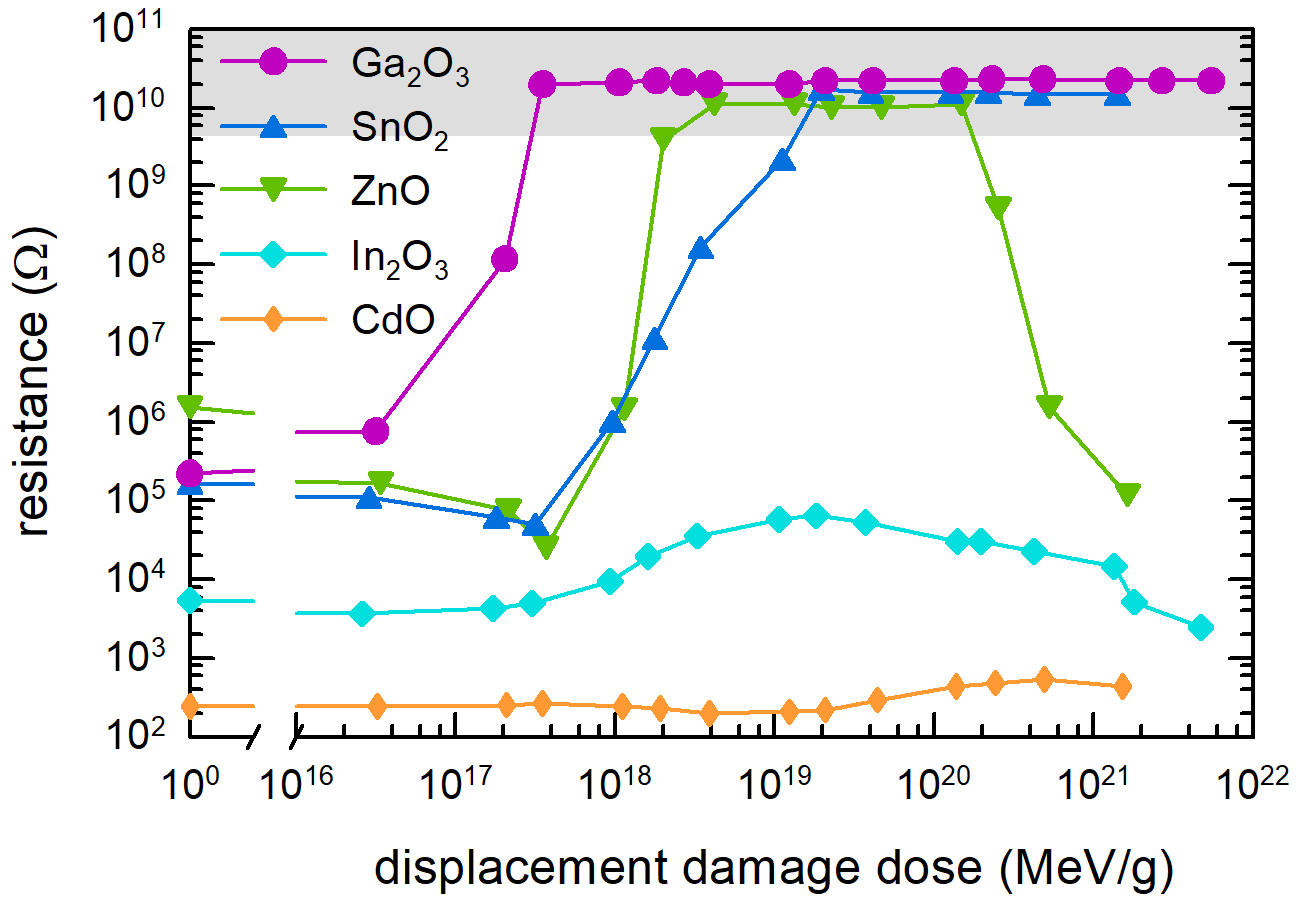
Within a collaboration between the University of Oslo, the University of Canterbury in Christchurch, the Centre de Recherche sur l' Hetero-Epitaxie et ses Applications (CNRS-CRHEA) in Valbonne and the Semiconductor Physics Group of the Universität Leipzig a meta-study on the native defect-induced Fermi level stabilization was conducted. For that, the prominent semiconducting metal oxides CdO, In2O3, β-Ga2O3, SnO2 and ZnO were ion-irradiated at cryogenic temperature and their electrical properties were determined as a function of the irradiation dose as depicted in the figure. For low and intermediate doses, the conductivity increases with increasing dose and follows general trends expected by the amphoteric defect model. Formation of defect complexes with multiple charge states must be taken into account to explain the resistivity decrease of In2O3 and ZnO observed for highest dosis. Here donor-like complexes have higher charge states than compensating acceptor-like complexes. Besides the fundamental physics revealed in the study we provide guidelines for implant isolation of these prominent semiconducting metal oxides. Our approach may be applied to other semiconductors to understand electrical material properties for irradiation doses that induce defect complexes rather than point defects in the cation and anion sub-lattices.
Further information is available at:
J. Borgersen, L. Vines, Y. Frodason, A. Kuznetsov, H. von Wenckstern, M. Grundmann, M. Allen, J. Zúñiga-Pérez, K. Johansen
Experimental exploration of the amphoteric defect model by cryogenic ion irradiation of a range of wide band gap oxide materials
J. Phys.: Condens. Matter 32 505701(2020)
Identification of LiNi and VNi acceptor levels in doped nickel oxide
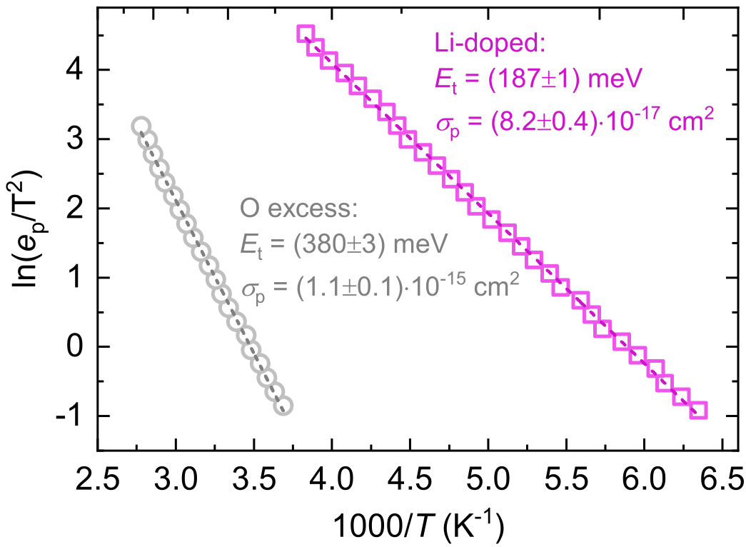
Nickel oxide is one of few transparent p-type semiconductors. P-type conduction originates from intrinsic nickel vacancies or from extrinsic dopants such as lithium being a substitutional cationic acceptor. The energetic position of these acceptors within the NiO bandgap has so far not been experimentally determined. We studied the charge transition levels (CTLs) of these acceptors experimentally by depletion layer spectroscopy within a vertical p-NiO/n++-SnO:F diode structure. The current rectification of these diodes is sufficient for thermal admittance and capacitance-voltage spectroscopy. For sample growth pulsed laser deposition was used and different conditions were employed to induce nickel vacancies or to incorporate lithium. For each sample a single defect level was observed. From Arrhenius-evaluation (see figure) the activation energy Ea (with respect to the valence band maximum) were determined to be 190 meV and 410 meV for the Li-doped and oxygen-rich sample, respectively. We attribute these defects to the (0/-) CTLs of the LiNi and the VNi acceptor, respectively.
Further information is available at:
R. Karsthof, H. von Wenckstern, V.S. Olsen, M. Grundmann
Identification of LiNi and VNi acceptor levels in doped nickel oxide
APL Materials 8, 121106 (2020)
Review on combinatorial material sysnthesis by pulsed-laser deposition

Combinatorial material synthesis has led to a significant acceleration in the optimization of solid state alloys. Two approaches to combinatorial material synthesis based on ablation of segmented ceramic targets during pulsed-laser deposition (PLD) were recently developed at Universität Leipzig and are shortly described in the current review. Azimuthally or radially segmented targets, as visualized in the figure, enable the creation of in-plane (lateral) and out-of-plane (vertical) continuous composition spreads, respectively. Radially segmented targets can additionally be used to synthesize a discrete binary material library.
Further information is available at:
Holger von Wenckstern, Max Kneiß, Anna Hassa, Philipp Storm, Daniel Splith and Marius Grundmann
A review of the segmented-target approach to combinatorial material synthesis by pulsed-laser deposition
phys. stat. sol. (b) 1900626 (2019)
Book chapters on PLD growth of and pn-diodes with Ga2O3 published
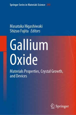
Springer Series in Material Science 293 focusses on the ultrawide bandgap semiconductor Ga2O3. The book entitled "Gallium Oxide Technology, Devices and Applications" was edited by Masataka Higashiwaki and Shizuo Fujita. We have contributed a chapter on the heteroepitaxial growth and basic material properties of binary β-Ga2O3 thin films. Further, these material properties are presented as a function of the alloy composition of ternary (In,Ga)2O3 and (Al,Ga)2O3, respectively. In a second chapter properties of various pn-heterodiodes to β-Ga2O3 are surveyed. We discuss current-voltage characteristics, the built-in potential obtained from capacitance-voltage measurements and finally break-down voltages for each material combination considered.
The book chapters are available at
Holger von Wenckstern, Daniel Splith, Marius Grundmann
Heteroepitaxial Growth of Ga2O3 and Related Alloys
In: Higashiwaki M., Fujita S. (eds) Gallium Oxide. Springer Series in Materials Science, vol 293 (Springer, Cham, 2020), Online ISBN
978-3-030-37153-1
TDaniel Splith, Peter Schlupp, Holger von Wenckstern, Marius Grundmann
All-Oxide pn-Heterojunction Diodes with β-Ga2O3
In: Higashiwaki M., Fujita S. (eds) Gallium Oxide. Springer Series in Materials Science, vol 293 (Springer, Cham, 2020), Online ISBN
978-3-030-37153-1
Low-voltage ring oscillators and high gain flexible inverters based on amorphous zinc tin oxide
Transparent and low-cost amorphous transistor technology has become an emerging market sentiment even though it is entirely based on indium-gallium-zinc-oxide (IGZO) active layers. Further, the unipolar circuitry is based on MISFET technology. However, there are viable alternatives to IGZO one of them is zinc-tin-oxide (ZTO) that consists of abundant elements, only. For ZTO we introduced Schottky diode FET logic that enables so far unprecented performance concerning subthreshold swing of individual MESFETs or peak gain maximum of inverters that were cascaded into ring oscillators with single stage delay times of 277 ns that can further be reduced by miniaturization of the current transistor layout with a gate width and length of 200mm and 3 mm, respectively. We further realized high-gain inverters on flexible substrates that utilize NiO/ZTO pn-junctions as gate diodes. These inverters operate properly after being bent at bending radii of 2mm.
Details about these transparent, room temperature fabricated circuit elements can be found at:
O. Lahr, S. Vogt, H. von Wenckstern, M. Grundmann
Low-Voltage Operation of Ring Oscillators Based on Room-Temperature-Deposited Amorphous Zinc-Tin-Oxide Channel MESFETs
Adv. Electron. Mater. 1900548 (2019)
The results of room temperature deposited inverters on flexible substrate are published at:
P. Schlupp, S. Vogt, H. von Wenckstern, M. Grundmann
Low voltage, high gain inverters based on amorphous zinc tin oxide on flexible substrates
APL Materials 8, 061112 (2020)
Properties of orthorhombic (In,Ga)2O3 thin films and Schottky barrier diodes thereon
The orthorhombic Ga2O3 polymorph has a large predicted spontaneous polarization making the
material very interesting for growth of heterostructures with exceptionally high two-dimensional electron density.
However, this polymorph is metastable and melt-growth of bulk crystals for homoepitaxy is not possible.
We have determined epitaxial relationships between orthorhombic (001)Ga2O3 and numerous substrate materials.
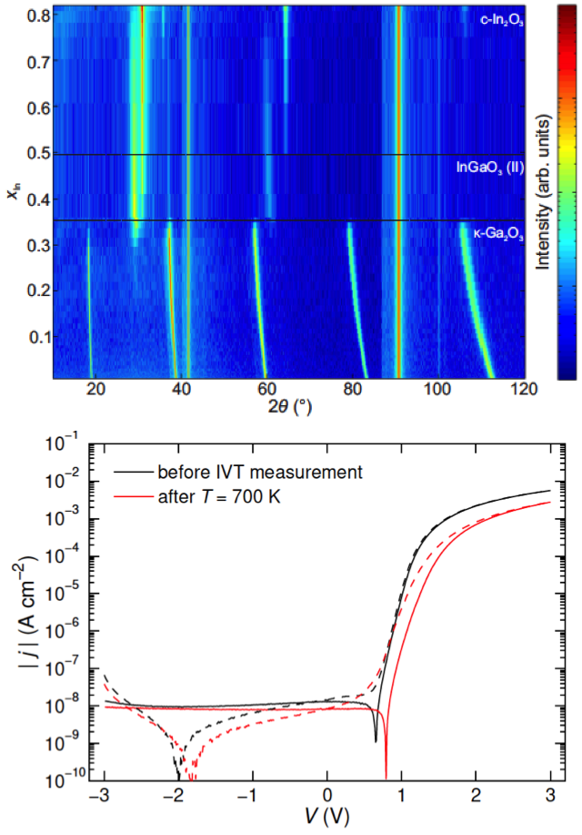
Further, ternary thin films with systematic lateral variation of the cation composition were realized
by pulsed-laser ablation of segmented targets, a chemical analysis is depicted in the figure.
The maximum indium content in orthorhombic gallium oxide was extended to 35%.
This allowed describing important material parameters, e.g. the band gap, latticing constant, etc.,
for a wide range of alloy compositions.Another highlight is the fabrication of the first Schottky barrier
diode to orthorhombic Ga2O3 which was enabled by increasing the free electron concentration by Zr doping demonstrating
that growth of semiconducting %kappa;-Ga2O3 thin films is feasible. The diodes are stable under high temperatures,
high rectification was maintained even after heat treatment at 700K (see figure).
Further information is available at:
A. Hassa, H. von Wenckstern, D.Splith, C. Sturm, M. Kneiß, V. Prozheeva and M. Grundmann
Structural, optical and electrical properties of orthorhombic κ-(InxGa1-x)2O3 thin films
APL Materials 7, 022525 (2019)
and
M. Kneiß, A. Hassa, D.Splith, C. Sturm, H. von Wenckstern, T. Schulz, N. Koch, M. Lorenz and M. Grundmann
Tin-Assisted PLD-Growth of κ-Ga2O3 Thin Films with High Crystalline Quality
APL Materials 7, 022516 (2019)
Properties of (In,Ga)2O3 alloys
For Elsevier's Metal Oxides series the book "Gallium Oxide Technology, Devices and Applications" was edited by Stephen Pearton, Fan Ren and Michael Mastro.
We have contributed a chapter covering the physical properties of (InxGa1-x)2O3 thin films.
We discuss growth methods, epitaxial relationships, structural, electrical as well as optical properties for the entire phase diagram. Further, properties of demontrator devices such as photo detectors are covered.
Samples, realized by a combinatorial material science approach, are used to identify growth conditions that are favorable for stabilization of a certain polymorph.
Further information is available at:
Holger von Wenckstern
Properties of (In,Ga)2O3 alloys
in: Gallium Oxide Technology, Devices and Applications, eds. Stephen Pearton Fan Ren Michael Mastro, Elsevier (2019), ISBN: 9780128145210
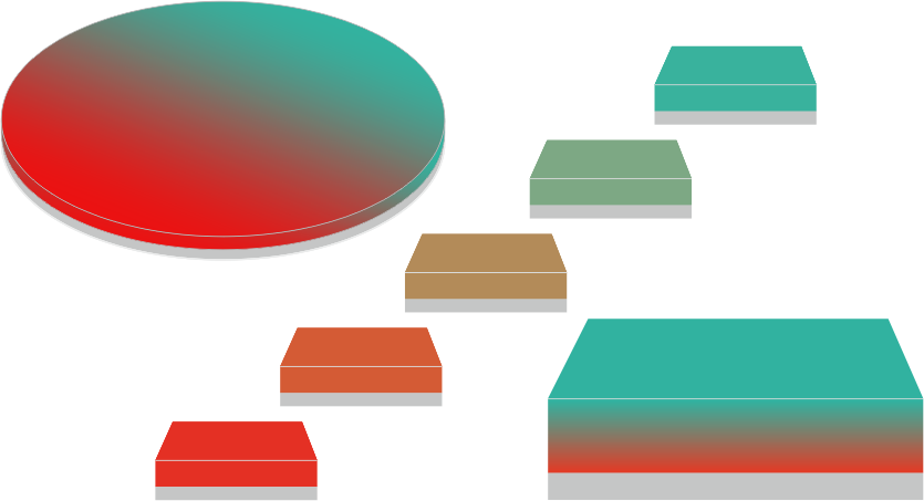
Combinatorial material science enabled by pulsed laser deposition using radially segmented targets
We introduce an approach allowing i) realization of discrete composition spread libraries and ii) deposition of samples with continuous composition spread in growth direction. For that, radially PLD
targets are manufactured in house and the shape of the inner segment resembles an ellipse. By controlling the position at which the laser radiation is incident on the radially segmented target a direct control
of the time averaged particle flux is possible. The larger the radial position of the incident radiation (cf. red dashed circles in the figure), the higher is the share of the material within the outer segment on the composition of the PLD plasma.
Discrete sample libraries can be created by deposition of homogeneous thin films for various fixed radial positions of the laser spot. Samples with composition gradient in growth direction are obtained by
variation of the radial laser spot position position during growth.
Further information is available at:
M. Kneiß, P. Storm, G. Benndorf, M. Grundmann and H. von Wenckstern
Combinatorial material science and strain engineering enabled by pulsed laser deposition using radially segmented targets
ACS Comb. Sci. 20, 643 (2018)
Influence of Oxygen Deficiency on the Rectifying Behavior of Transparent-Semiconducting-Oxide-Metal Interfaces
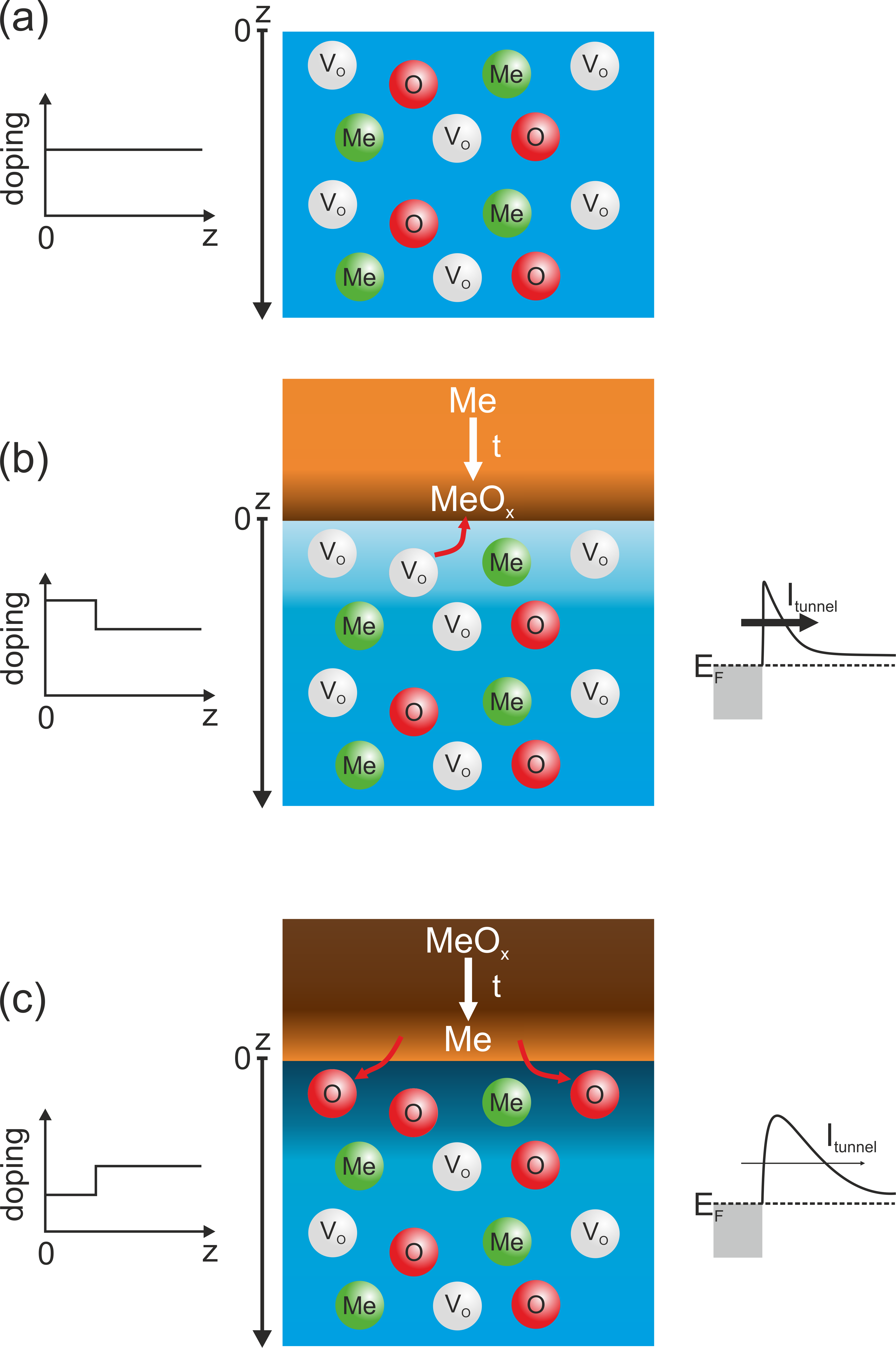
The formation of Schottky barrier diodes (SBD) is prerequisite for several device applications including rectifiers, photo detectors
and metal-semiconductor field-effect transistors. Concerning transparent semiconducting oxides the realization of high-quality
SBDs is commonly not straight forward. Typically, oxygen plasma surface treatment and/or reactive sputtering of the contact metal
is required for high rectification. On the basis of X-ray photoelectron spectroscopy and electrical transport measurements we demonstrate the mechanism leading to high-quality SBDs in case of reactively sputtered contacts to
zinc-tin oxide. Results are compared to reference diodes realized by non-reactive sputter deposition.
Further information is available at:
Thorsten Schulz, Sofie Bitter, Peter Schlupp, Holger von Wenckstern, Nobert Koch, Marius Grundmann
The influence of oxygen deficiency on the rectifying behavior of transparent semiconducting oxide-metal interfaces
Phys. Rev. Appl. 9, 064001 (2018)
Group-III Sesquioxides: Growth, Physical Properties and Devices
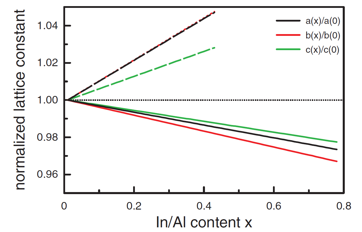
The group-III sesquioxides find potential application as high-power devices or solar-blind UV detectors. For each binary technology for growing
single-crystalline bulk material exists, enabling homoepitaxial growth of thin films with high crystalline quality. The bandgap can be tuned in an
energy range from about 4 to 8 eV for the ternary alloys and allows growth of heterostructures with large band offset. In this current review past
results and recent investigations on the growth, the material properties, contact fabrication and the alloying of group-III sesquioxides are reviewed,
and an overview on demonstrator devices is provided. The variation of the lattice constants within monoclinic (InxGa1-x)2O3
and (AlxGa1-x)2O3 is shown examplarily in the figure.
Further information is available at:
Holger von Wenckstern
Group-III Sesquioxides: Growth, Physical Properties and Devices
Adv. Electron. Mater. 3, 1600350 (2017)
The Vital Role of Oxygen for the Formation of Highly Rectifying Schottky Barrier Diodes on Amorphous Zinc-Tin-Oxide with Various Cation Composition
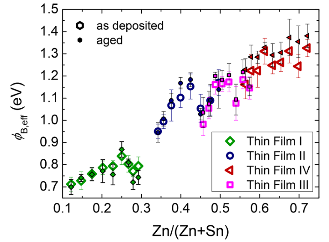
Amorphous, low-temperature deposited semiconducting oxides drive pixel elements of active matrix displays. Up to now, layers containing indium and
gallium are used for these application. In order to reduce material costs a substitution of these elements by abundant metals is desired. Zinc-tin-oxide
is a promising substitute with promising properties even if deposited at room temperature. We describe properties of reactively sputtered platinum
Schottky barrier diodes on zinc-tin-oxide thin films with laterally varying cation composition, which were grown by a continuous composition spread technique
for pulsed laser deposition (see below). We found that the rectification of the diodes increases with increasing zinc content and saturates for a zinc content of
about 0.4 and higher. The effective barrier height increases monotonously as visible in the figure. Further we could show, that the amount of oxygen offered during contact deposition is essential for the rectification and long-term stability
of the diodes.
Further information is available at:
Sofie Bitter, P. Schlupp, H. von Wenckstern, M. Grundmann
The Vital Role of Oxygen for the Formation of Highly Rectifying Schottky Barrier Diodes on Amorphous Zinc-Tin-Oxide with Various Cation Composition
ACS Materials and Interfaces 9, 26574-26581 (2017)
Method of choice for fabrication of high-quality β-gallium oxide-based Schottky diode
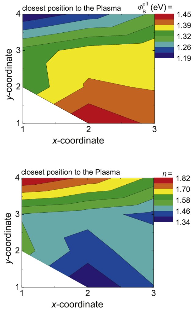
Gallium oxide is has for a semiconductor a very large bandgap of about 4.9 eV in its most stable monoclinic modification. This renders the material
eminently suited for high-power applications. Rectifying Schottky barrier diodes represent the basic high-power device. We report on properties of
differently deposited platinum Schottky diodes on Ga2O3 thin films grown heteroepitaxially by pulsed laser deposition on (00.1) Al2O3 substrates.
High Schottky barrier height and low ideally factor is obtained for thermally evaporated metal layers. For sputtered contacts, reactive sputtering
leads to higher barriers than for non-reactively or evaporated diodes. Further, long-distance sputtering results in higher Schottky barriers and lower
ideality factor compared to sputter processes with much lower target-to-substrate distance. This effect is impressively illustrated by a peripheral
sputter process resulting in a variation of the target-to-substrate distance on one thin film. As the figure demonstrates lower distances result
in inferior diode properties due to stronger defect formation by the impinging of higher energetic particles.
Further information is available at:
Stefan Müller, Holger von Wenckstern, Florian Schmidt, Daniel Splith, Heiko Frenzel, Marius Grundmann
Method of choice for fabrication of high-quality β-gallium oxide-based Schottky diodes
Semic. Sci. Technol. 32, 065013 (2017)
Ring Oscillators based on ZnO Channel JFETs and MESFETs
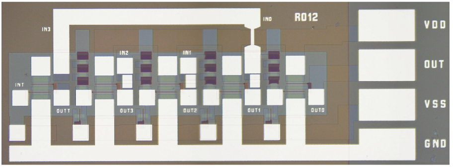
Electronic circuits based on oxide semiconductors find application in active matrix displays and present an essential ingredient to future transparent
and possibly flexible circuitry. Most approaches are based on metal-insulator-semiconductor gate structures that typically have extremely low leakage
current densities. However, Schottky diodes to wide bandgap oxide semiconductors have barrier height of 1eV and higher and therefore very low leakage current
density as well. The same holds true for all-oxide pn-heterodiodes that can be used to control the source-drain current of field-effect transistors.
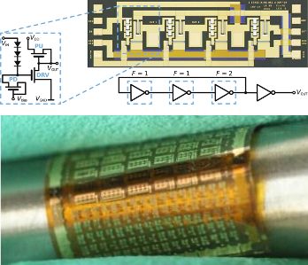
In the current manuscript we implemented Schottky barrier diodes and pn-heterodiodes as gate contacts to ZnO-based inverters used as building blocks of
ring oscillators; the design is depicted in the image. We demonstrated single stage delay times down to 110 ns and very low power consumption.
Further information is available at:
F.J. Klüpfel, H. von Wenckstern, M. Grundmann
Ring Oscillators based on ZnO Channel JFETs and MESFETs
Adv. Electr. Mater. 2, 1500431 (2016)